How do scientists take breathtaking 3D photos of viruses and insect eyes?
Prompted by A NerdSip Learner
Understand how electron beams reveal the nanoscale world.
Have you ever tried to paint a tiny masterpiece using a giant, thick brush? That is essentially what happens when we try to look at nanoscale objects using regular light. The "brush" (the wavelength of visible light) is simply too big to paint the fine details!
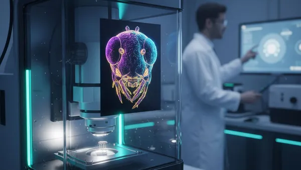
Scanning Electron Microscopy (SEM) solves this by swapping light for a beam of electrons. Because electrons have a wavelength up to 100,000 times shorter than visible light photons, they act like an ultra-fine pen. This allows SEMs to achieve resolutions down to 1 nanometer—small enough to see the individual strands of DNA or the intricate geometry of a virus.
But an SEM doesn't take a single snapshot. Instead, it raster scans. Imagine standing in a pitch-black room with a tightly focused flashlight. By sweeping the beam left to right, line by line, you can map out everything in the room. The microscope does exactly this, measuring the electrons that bounce off the sample to build a stunning, hyper-detailed, three-dimensional image of the microscopic world.
Key Takeaway
SEMs use electron beams with ultra-short wavelengths to map surfaces line-by-line, revealing nanoscale details that visible light cannot capture.
Test Your Knowledge
Why can an SEM reveal much smaller details than a standard optical microscope?
When the SEM's electron beam strikes your sample, it doesn't just bounce back in one way. It creates a splash of different microscopic signals. Scientists act as detectives to decode the two main types of returning electrons.
First, we have Secondary Electrons (SE). These are low-energy particles knocked loose right at the surface of the sample. Because they come from the very top layer, they give us a highly detailed, 3D map of the object's topography (its physical texture and shape). If you want to see the microscopic hairs on a spider's leg, secondary electrons are your best friend.
Then, we have Backscattered Electrons (BSE). These are the original beam electrons that plunge deeper into the sample and ricochet back out like high-speed billiard balls. Heavier elements (like iron) bounce back more electrons than lighter ones (like carbon). In a BSE image, heavier elements glow brighter, allowing you to instantly map the chemical composition of the object you are looking at!
Key Takeaway
Secondary electrons reveal physical surface texture, while backscattered electrons highlight chemical differences based on atomic weight.
Test Your Knowledge
If you wanted to map the physical shape and texture of a microchip's surface, which signal would be most useful?
You can't just toss a living bug into an SEM and press a button. Preparing a sample for this extreme machine requires two crucial steps: surviving a vacuum environment, and getting "blinged out."
First, the inside of an SEM must be a high vacuum. If there were standard air molecules inside the chamber, the electron beam would crash into them and scatter, completely ruining the image. Because of this intense vacuum, wet or living biological samples must be completely dried out first, otherwise the rapid pressure change would destroy them.
Second, the sample needs to be electrically conductive. If you blast a non-conductive object (like a dried insect or a piece of plastic) with negatively charged electrons, the charge builds up on the surface. This causes a blinding white glare in the image known as "charging." To prevent this, scientists blanket the sample in an ultra-thin layer of pure gold or platinum, giving the electrons a safe, conductive path to flow.
Key Takeaway
SEM samples must be placed in a vacuum so the beam doesn't scatter, and non-conductive items are coated in a metal like gold to prevent static buildup.
Test Your Knowledge
Why are non-conductive biological samples typically coated in a thin layer of gold before being placed in an SEM?
Track your progress, earn XP, and compete on leaderboards. Download NerdSip to start learning.