Could the sand beneath your feet power the world’s most advanced computers?
Prompted by A NerdSip Learner
Master the complete journey from raw silica to silicon chips.
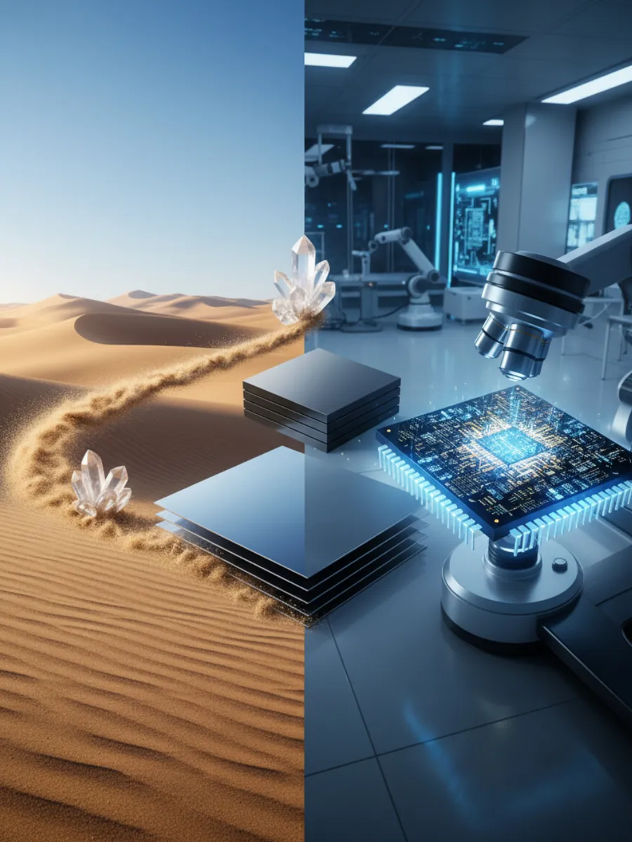
Believe it or not, the super-brain inside your laptop starts its life as common sand! Sand is composed mostly of silicon, the second most abundant element in the Earth's crust. But we can't just shovel sand into your computer case.
First, we have to purify it. Imagine trying to bake the perfect cake, but the flour has to be 99.9999% pure. Scientists melt the sand down to remove impurities, leaving behind a hot, molten liquid. From this liquid, they grow a giant, single crystal called an ingot.
This ingot looks a bit like a massive, shiny metal sausage. Once it cools, it is sliced into incredibly thin, circular discs called wafers. These wafers serve as the polished canvas where the magic happens. It is on these discs that we build the microscopic cities that power our digital world!
Key Takeaway
Computer chips begin as purified sand formed into thin discs called silicon wafers.
Test Your Knowledge
What is the primary raw material used to create the silicon ingot?
Now that we have our blank silicon wafer, how do we draw the complex circuitry? We don't use a pen; the lines would be way too thick! Instead, engineers use a process called photolithography. Think of it like stenciling with light.
First, the wafer is coated with a light-sensitive liquid called 'photoresist.' Then, ultraviolet light is shone through a mask—which is essentially a high-tech stencil containing the blueprint of the chip.
Wherever the light hits the wafer, the chemical coating hardens. The soft parts that were hidden in the shadow are washed away, leaving a specific pattern on the silicon. This process is repeated dozens of times, layer by layer, to build a complex structure. It’s like 3D printing, but on a microscopic scale using light beams!
Key Takeaway
Engineers use light and stencils to 'print' circuit patterns onto the silicon wafer.
Test Your Knowledge
What tool is used to transfer the circuit pattern onto the wafer?
Once the patterns are etched onto the wafer, we treat the silicon with different gases and metals to change how it conducts electricity. This creates transistors.
To understand a CPU, you just need to understand the transistor. It is simply a microscopic light switch. It has two states: On (represented as 1) and Off (represented as 0). By combining these 1s and 0s, computers can do math, display photos, and play movies.
A modern CPU contains billions of these tiny switches packed into an area the size of a fingernail. Finally, the large wafer is sliced up into individual square chips (called dies). The working chips are placed into that protective metal and plastic square you see when you build a PC. From sand to a super-switch, that is how a CPU is born!
Key Takeaway
A CPU is essentially made of billions of microscopic on/off switches called transistors.
Test Your Knowledge
What is the basic function of a transistor inside a CPU?
Track your progress, earn XP, and compete on leaderboards. Download NerdSip to start learning.